The copyright of this article belongs to Siansonic Technology.The production is prohibited without permission.
"Apart from lithography machines, photoresists are a major 'roadblock' in high-end chip fabrication." Clearly, photoresists, as specialized materials in the chip-making phase, hold a pivotal status in the semiconductor world.
Photoresist is a type of photosensitive polymer liquid, also known as a photo-etching agent. Its solubility changes under exposure to ultraviolet light, electron beams, ion beams, or X-rays. This property is harnessed to etch patterns. The early development of photoresists is deeply intertwined with the advent of photography in the early 19th century. The first permanent “photos” were essentially lithographic images created by projection printing. Around 1826, Joseph Niépce pioneered photography. He used a polished tin plate, coated with a tar-like photoresist called “Judea bitumen,” to capture an image of his courtyard. Exposed to sunlight, the Judea bitumen became less soluble. The development process removed unexposed areas, revealing the substrate beneath. The image was then permanently etched onto the exposed tin surface with acid. This process bears striking resemblance to the techniques used today in fabricating the most complex microelectronic devices.

Figure 1.Semiconductor wafers for ultrasonic coating photoresist
However, Judea bitumen was not the ideal photo-etching agent due to its limited photosensitivity, requiring prolonged exposure to capture images. This led to the development of more sensitive photoresist systems based on "Dichromated Gelatin" (DCG). DCG proved to be a highly successful imaging material, sparking the rise of the entire lithography industry in the mid-19th century. Throughout the 20th century, the production of printing plates remained almost exclusively the domain of DCG photoresists. However, they fell short of meeting the needs of IC manufacturing. The gelatin lacked the resistance required for certain acid etching processes essential for IC structures. Furthermore, DCG photoresists in all applications were constrained by "dark reactions." This means once prepared, even in complete darkness, DCG photoresists would undergo cross-linking reactions, leading to degradation after just a few hours of storage. This necessitated the search for alternatives to gelatin-based etching agents. The evolution of photoresists has been driven by varying applications and demands, making the ongoing research and development of photoresists a significant topic in the field of technology.
Photoresist is a specialized material, recognized as one of the eight essential core materials in semiconductor fabrication. Simply put, lithography is a technique that maps integrated circuits onto silicon wafers using special light. Photoresist serves to protect the silicon wafer from any other damages. During lithography, ultrasonic photoresist coating forms a corrosion-resistant layer on the silicon wafer's surface. Then, using selective etching techniques, intricate circuit patterns required on the silicon wafer are obtained. The precision of these patterns dictates the lithography process, with the photoresist composition precisely tailored to meet specific requirements.
Photoresists typically consist of a light-sensitive mixture of photopolymer (polymerizer), sensitizer (photo-initiator), solvent, and additives. The photopolymer binds various materials together, forming the photoresist's framework. It determines the basic attributes of the photoresist such as hardness, flexibility, and adhesion. The sensitizer defines the photoresist's sensitivity and resolution. Solvents, forming the largest proportion in photoresist, maintain its liquid state. Additives alter specific chemical properties of the photoresist. A superior photoresist should exhibit high resolution, high contrast, and high sensitivity, ensuring the precise and faithful transfer of intricate patterns from the mask to the silicon wafer. The quality and performance of photoresists directly impact the chip's performance, yield rate, and reliability.
In the chip manufacturing process, lithography encompasses numerous steps and represents 45% of the entire workflow. A key time factor lies in the precision handling of ultrasonic photoresist coating and lithography machines. Ultrasonic photoresist coating, with its distinct advantages, ultrasonic photoresist coating has emerged as a leading technique in applying photoresists. In comparison to traditional spin coating methods, ultrasonic photoresist coating significantly minimizes photoresist waste, thus offering substantial cost savings. Additionally, it facilitates coating on structured silicon wafers, a task previously challenging.

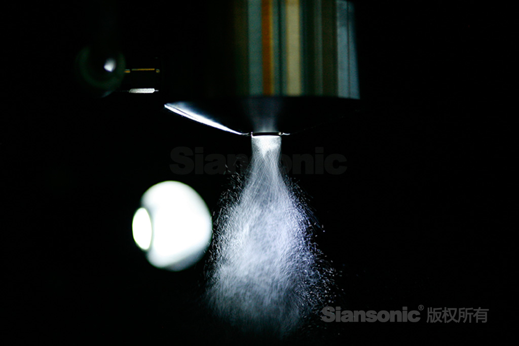
Figure 2.Conemist nozzle for photoresist spray coating
Siansonic Technology with its nearly 40 years of expertise in piezoelectric and ultrasonic technologies, excels in the field. Centered around advanced ultrasonic spray coating technology, the company's products are extensively used in ultrasonic photoresist coating applications. Siansonic Technology plays a pivotal role in advancing the semiconductor sector's ultrasonic photoresist coating techniques.